pages

Infrared Fire-Cracker Igniter

Firecrackers are normally ignited by using a matchstick or a candle. You have to run away quickly after igniting the fuse of the firecracker. This method of igniting firecracker is unsafe, because the danger of the firecracker bursting before you reach a safe distance is always there. The device described here uses remote control, usually used with TV receivers or CD players, to burst the fire-cracker. Thus the firecracker can be ignited from a safe distance using the circuit described below in conjunction with the remote control.

In the diagram shown here, normally the output of IC1 is low and green LED2 is ‘on’ and the red LED3 ‘off.’ This indicates that the circuit is ready for use. When any key on the remote control is pressed, output pin 3 of IRX1 (IR receiver module TSOP1738) goes low. This output is connected to pin 2 of IC1 via LED1 and resistor R4 to trigger the monostable operation of IC1. The output of IC1 remains high for a period equal to 1.1×R2×C2. With the values of the components given in the circuit diagram here, the period works out to 3.5 seconds approximately.

Infrared Fire-Cracker Igniter
Infrared Fire-Cracker Igniter Circuit Diagram

This activates relay RL1 and red LED3 glows and green LED2 turns off. ‘On’ state of red LED3 indicates that the firecracker is about to burst. R7 is a small part of the element of an electric heater (220V, 1000W), which is kept away from the electronic circuit and connected to the relay contacts through a thick electric cable. The resistance value of short length of the heater element (R7) is 3 to 3.5 ohms. A current of around 4 amperes flows through it when connected to a 12V battery. Flow of 4A current through R7 for 3.5 seconds makes it red hot, which ignites the fire-cracker.

The circuit is powered by a 12V, 7AH battery. IC2 provides about 9V for the operation of the circuit. The circuit should be housed in a metallic cabinet to prevent it from being damaged by bursting of the firecracker. The IR receiver and the two LEDs should be fixed on the front panel of the cabinet. Wiring and relay used in the circuit should be chosen such that they are able to carry more than 5 amperes of current.
Author: Pardeep Vasudeva - Copyright: EFY Mag

High Level Wideband RF Preamplifier

A linear RF amplifier can be made in two ways: (1) with the aid of a linear active element, or (2) with a non-linear element operating with negative feed-back. This circuit is of the second kind, using an RF power transistor as the active element. Feedback is also required to ensure correct termination (50 Q) of the aerial, since bipolar transistors normally exhibit a low input impedance. Also, the noise figure is not increased because virtually no signal is lost.

High Level Wideband RF Preamplifier Circuit Diagram

The common-base amplifier is based on a UHF class A power transistor Type 2N5109 from Motorola. The feedback circuit is formed by RF transformer Th. The input and output impedance of the preamplifier is 50 4 for optimum perform-ance. Network R3-C5  may have to be added to  preclude oscillation outside the pass-band, which  ranges from about 100 kHz to 50 MHz. The gain is  approximately 9.5 dB, the noise figure is between 2  and 3 dB, and the third-order output intercept point  is at least 50 dBm.
The input/output transformer is wound on a Type FT37-75 ferrite core from Micrometals. The input winding is 1 turn, the output winding 5 turns with a tap at 3 turns.

Source:Ecircuitslab.com

How to Build a UPS for USB devices

Portable systems often include circuitry that derives power from an external source, such as USB. When the system disconnects from the USB supply, a battery takes over and supplies current via a dc/dc converter. A diode-OR connection (Figure 1 offers the easiest way to ensure that the supply voltage doesn't sag during this switchover to the battery. The diode's forward voltage drop, however, can reduce battery life and efficiency.

How to Build a UPS for USB devices
A diode-OR connection is effective but lossy.


How to Build a UPS for USB devices
 A boost-converter circuit is an improvement over the simple diode-OR connection.

The single-cell, boost-converter circuit with external PFET (Figure 2) is an improvement over the diode-OR connection. The PFET, Q1, coupled with IC1's internal gain block, forms a linear regulator. The USB power supply has a diode-OR connection to Q1's source. Setting the boost converter's output to 3.4V allows the drain of Q1 to regulate to 3.3V. This configuration produces negligible loss in Q1. The bus-supply voltage available to USB devices ranges from 4.4 to 5.25V.

When you connect the bus, it forward-biases D1 and causes the boost converter to idle. The converter continues to idle as long as its output remains above the 3.4V regulation point. The bus supply serves the load and activates the current source to charge the battery.


How to Build a UPS for USB devices

Adjusting R1 allows you to set the current-source output to charge the nickel-metal-hydride cells at a level one-tenth the battery's capacity. Disconnecting the circuit from the USB supply causes the boost converter to cease idling and supply current to the load via the battery. Figure 3 shows that the load current suffers no interruption during a switchover from USB to battery.

How to Build a Shake Tic Tac LED Torch

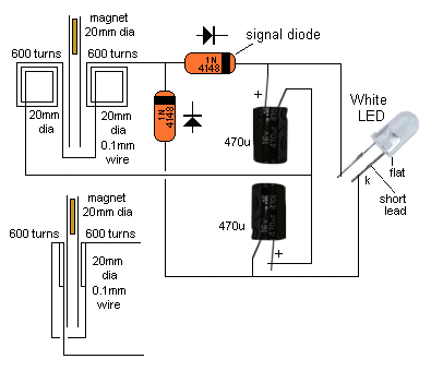
In the diagram, it looks like the coils sit on the “table” while the magnet has its edge on the table. This is just a diagram to show how the parts are connected. The coils actually sit flat against the slide (against the side of the magnet) as shown in the diagram:

How to Build a Shake Tic Tac LED Torch


 Shake Tic Tac LED Torch Circuit Diagram

The output voltage depends on how quickly the magnet passes from one end of the slide to the other. That's why a rapid shaking produces a higher voltage. You must get the end of the magnet to fully pass though the coil so the voltage will be a maximum. That’s why the slide extends past the coils at the top and bottom of the diagram.

The circuit consists of two 600-turn coils in series, driving a voltage doubler. Each coil produces a positive and negative pulse, each time the magnet passes from one end of the slide to the other.
The positive pulse charges the top electrolytic via the top diode and the negative pulse charges the lower
electrolytic, via the lower diode.

The voltage across each electrolytic is combined to produce a voltage for the white LED. When the combined voltage is greater than 3.2v, the LED illuminates. The electrostatics help to keep the LED illuminated while the magnet starts to make another pass.